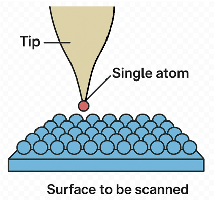
Scanning tunnelling microscopy (STM) is a high-resolution imaging technique that maps a sample’s surface structure by measuring electron tunnelling between a sharp metal tip and the sample.
STM enables the imaging, manipulation, and characterisation of materials at the atomic scale. Invented in 1981 by Gerd Binnig and Heinrich Rohrer at IBM Zurich, for which they received the 1986 Nobel Prize in Physics, STM marked the beginning of modern nanotechnology. Unlike optical or electron microscopes, which rely on the reflection or transmission of light or electrons, STM measures a quantum mechanical current that flows through a vacuum gap between a sharp conductive tip and a conducting or semiconducting surface. This unique approach allows STM to resolve individual atoms and probe their electronic properties.
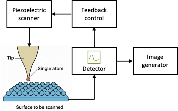
A typical STM system comprises several key components: a sharp metallic tip, a piezoelectric scanner, a feedback control system, and associated electronics for current detection and image acquisition (see diagram below). Each plays a crucial role in achieving atomic-scale precision.
The STM tip must be atomically sharp, ideally terminating in a single atom, because the tunnelling current is dominated by the atom closest to the sample. It is usually made of tungsten, platinum–iridium, or another conductive material. Tips are often prepared by electrochemical etching, which produces a fine point, followed by gentle cleaning to remove contaminants.
When the tip is brought extremely close — on the order of a nanometre — to a conductive surface and a fixed bias voltage is applied between them, the probability of electrons tunnelling through the vacuum barrier varies with the length of that barrier. Since an electric current is defined as the net flow of electric charge, the successful tunnelling of electrons through the barrier gives rise to a current :
where is the transmission probability and
is the number of incident electrons per unit time.

Question
What is the purpose of introducing a bias voltage between the tip and the surface?
Answer
When no bias voltage is applied, the circuit containing the tip and the surface is in thermodynamic equilibrium, with both tip and surface sharing the same electrochemical potential. At this equilibrium, the probability of electrons tunnelling from the tip to the surface is equal to the probability of tunnelling from the surface to the tip, resulting in no net electron flow.
When a non-zero bias voltage is applied, the tip and the surface are held at different potentials. This application of voltage introduces a thermodynamic driving force in the circuit by shifting the entire electronic structure of the surface (valence band, conduction band and Fermi level) as a rigid block by relative to the that of the tip. The tunnelling probability then becomes greater in one direction, creating a net electron flow. In essense, the bias voltage creates the energy difference between the tip and the surface required to generate a measurable tunnelling current.
Notably, the direction of electron flow depends on the polarity of the bias voltage:
-
- Positive surface bias (
): Electrons tunnel from the tip’s occupied states into the surface’s unoccupied states.
- Positive surface bias (
-
- Negative surface bias (
): Electrons tunnel from the surface’s occupied states into the tip’s unoccupied states.
- Negative surface bias (
An STM experiment can be performed in two distinct modes: constant-height or constant-current. The choice between modes depends on the sample’s roughness and conductivity, as well as the desired imaging speed.
In the constant-height mode, the feedback loop, consisting of a proportional–integral–derivative (PID) controller, is briefly engaged at the start to bring the tip to the initial tunnelling distance. The desired constant height is established by moving the tip until the setpoint current is reached, after which the loop is disabled.
The movement of the tip relative to the sample is controlled via a piezoelectric scanner, usually a ceramic tube or stack, that expands or contracts linearly in response to applied voltages. This scanner allows sub-ångström precision in all three spatial directions (x, y, and z). During scanning in the constant-height mode, the x– and y-voltages move the tip laterally across the surface. When the tip passes over a higher region of the surface (closer to atoms), the effective barrier distance decreases, and the tunnelling current increases sharply; when it passes over a lower region (further from atoms), the distance increases slightly and current decreases. This variation in current reflects the surface topography.
In the constant-current mode, the feedback loop maintains the set tunnelling current by adjusting the z-position of the tip. The PID controller compares the measured current with a predefined setpoint and modifies the vertical voltage accordingly as the tip moves in the x– or y-directions, with the resulting z-signal representing surface height.
Finally, the varying current or voltage is processed by highly sensitive amplifiers and low-noise electronics. The resulting amplified signal is then analysed by computer software to generate topographic maps, which are often displayed as three-dimensional images (see diagram below).
Modern STM systems can also perform spectroscopic measurements, leading to scanning tunnelling spectroscopy (STS). In this mode, the tip is positioned over a fixed point on the surface and the feedback loop is turned off to maintain a constant tip height. The bias voltage between the tip and the surface is then varied, while the tunnelling current is recorded as a function of the applied voltage.
As mentioned in the above Q&A, varying the bias voltage shifts the electronic structure of one electrode as a rigid block relative to the other. As the positive surface bias increases, electrons in the tip can tunnel into unoccupied electronic states of progressively higher energy in the surface. By analysing how the tunnelling current changes with voltage , STS reveals the relative number of states available for tunnelling at each energy level. Peaks in the
versus
spectrum correspond to discrete energy levels, much like the features observed in optical or photoemission spectroscopy. The higher the peaks, the greater the density of states.
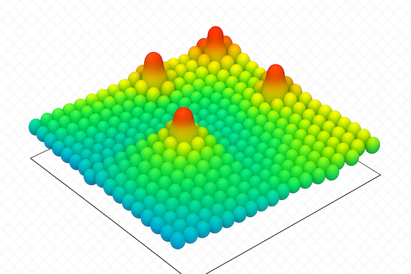
STS is often used to study crystal and semiconductor surfaces. For example, when a germanium crystal is cut (e.g. into Ge(111)), the surface atoms — originally tetrahedrally bonded in the bulk — find themselves missing some of their bonding partners, creating energetically unfavourable “dangling bonds”. To reduce surface energy, the atoms near the surface spontaneously rearrange, forming a stable periodic structure that differs from the bulk lattice.

During this surface reconstruction, some atoms known are displaced upwards to become adatoms, which sit above the surface layer (see diagram above). Other atoms, known as rest atoms, are not displaced upwards, but lose their original bonds and relocate slightly from their original positions on the surface.
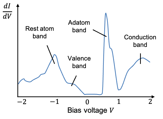
Although both adatoms and rest atoms possess dangling bonds, their electronic environments differ. Rest-atom dangling-bond states lie at lower energy because rest atoms are more strongly bound to the underlying crystal. These states tend to be occupied by electrons. In contrast, adatom dangling-bond states lie at higher energy owing to their weaker bonding to the substrate, and thus remain unoccupied. Consequently, in an STS measurement we observe a strong adatom peak at positive surface bias (electrons tunneling from tip to surface into empty adatom states) and a weaker rest-atom peak at negative bias (electrons tunneling from occupied rest-atom states into the tip).
Thus, the STS spectrum (see diagram below) provides direct insight into the nature of the surface atoms and their electronic states, and it serves as an important tool for validating theoretical surface reconstruction models.
In conclusion, the standard function of an STM is to image surfaces at atomic resolution. However, when operated under varying bias voltages, it can probe the electronic properties of the surface as a function of energy, becoming a spectroscopic technique.