Molecular Orbital (MO) theory states that electrons in a molecule occupy orbitals that span the entire molecule rather than being localised between atoms.
The theory was developed by Friedrich Hund, Robert Mulliken, John Slater and John Lennard-Jones, who proposed that when atoms approach each other to form a molecule, their atomic orbitals overlap and combine mathematically to generate new orbitals called molecular orbitals. This process is known as the linear combination of atomic orbitals (LCAO). In this approach, molecular orbitals are constructed by combining the wavefunctions of the contributing atomic orbitals, analogous to the superposition of waves.
Because each atomic orbital (AO) is described by a wavefunction, the MO wavefunction can be expressed as the sum or difference of the AO wavefunctions. For example, the MO wavefunction of H2 can be written as:
where and
are the 1s AO wavefunctions of the two hydrogen atoms.
Eq10 represents an approximate solution to the time-independent Schrödinger equation for the H2 molecule. An equally valid solution is
Since each AO can accommodate a maximum of two electrons, the orbital conservation principle of MO theory states that the total number of MOs formed must equal the total number of AOs combined to produce them. Incidentally, the two solutions for H2 correspond to different types of MOs: the addition of wavefunctions produces a bonding MO, while their subtraction produces an anti-bonding MO.

Bonding MOs are formed when the overlapping wavefunctions of AOs are in-phase, which leads to constructive interference, and hence a build-up of electron density between the bonding nuclei (see above diagram). The positively-charged nuclei are attracted to the region of higher electron density, resulting in a more stable system. Consequently, a bonding MO has a lower energy than the AOs from which it is formed.
Anti-bonding MOs, denoted by an asterisk (*), are due to the overlapping wavefunctions of AOs being significantly out-of-phase, which results in destructive interference, and therefore a node, between the bonding nuclei. The nuclei are attracted to the non-nodal electron densities, away from the internuclear region. This causes a destabilisation of the system (if the MO is occupied) and the anti-bonding MO having a higher energy than the AOs from which it is formed.
Besides bonding and anti-bonding MOs, a third type, called a non-bonding MO, can appear in molecules that have lone pairs of electrons. For example, in the hydroxyl radical ⋅OH, the hydrogen 1s AO overlaps with the oxygen 2pz AO to form a bonding MO and an anti-bonding MO, while the oxygen 2px and 2py AOs, which do not interact significantly with hydrogen due to symmetry, form a pair of degenerate (same energy) non-bonding MOs.
In general, non-bonding MOs are formed when the overlapping wavefunctions of AOs are partially out-of-phase. A non-bonding MO shows neither charge depletion nor charge accumulation between the nuclei. Electrons in such an MO neither contribute to nor reduce bond strength. Therefore, it has approximately the same energy as the AOs from which it is formed.
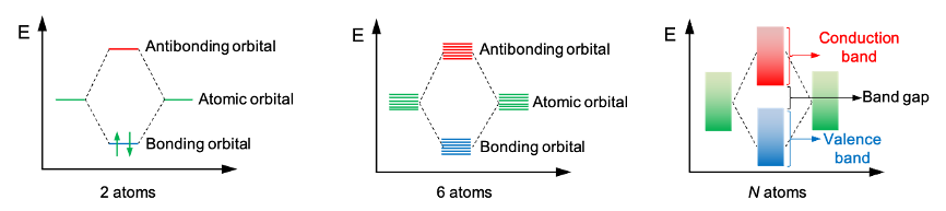
The relative energies of MOs and the AOs that form them are illustrated using molecular orbital diagrams. These diagrams typically consist of three columns of orbitals (see diagram below). The middle column contains MOs, while the left and right columns show the valence AOs of the atoms that combine to form the MOs. Horizontal lines represent the energy levels of the orbitals, and dotted lines link the MOs to the AOs used to construct them. Each MO has a characteristic symmetry, such as ,
or
.
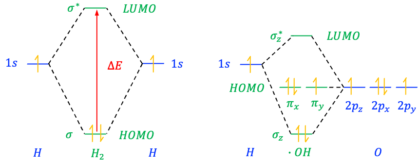
Electrons fill molecular orbitals according to the same rules used for atomic orbitals. They follow the Aufbau Principle, filling lower-energy orbitals before higher ones, and obey the Pauli Exclusion Principle, which states that no two electrons in the same orbital can have identical quantum numbers. Furthermore, Hund’s Rule, which states that electrons occupy degenerate orbitals singly before pairing, also applies. In the ground state configuration, the highest occupied molecular orbital (HOMO) of a molecule contains the highest-energy electrons. Electrons in the HOMO are the most likely to be donated in chemical reactions, such as nucleophilic reactions or excitation to higher orbitals. In contrast, the lowest unoccupied molecular orbital (LUMO) is the lowest-energy molecular orbital that is unoccupied by electrons. It is the orbital that accepts electrons during chemical reactions, such as electrophilic attack or electronic excitation. Together, the HOMO and LUMO are known as frontier orbitals.

Question
Why are the 2p AO energies of oxygen lower than the 1s AO energy of hydrogen in the hydroxyl radical?
Answer
This is mainly because oxygen has a much higher effective nuclear charge than hydrogen. The stronger positive charge of the oxygen nucleus is only partially shielded by its inner electrons. As a result, the valence electrons of oxygen experience a stronger attraction to the nucleus, which lowers the energy of its orbitals relative to the 1s orbital of hydrogen. The actual energy levels of the orbitals can be calculated using iterative computational techniques such as the Hartree self-consistent field method.
MO theory also introduces the concept of bond order, which helps predict the strength and stability of a bond. It is defined as:
where and
are the number of electrons in the bonding MO and the anti-bonding MO respectively.
A higher bond order indicates a stronger and more stable bond, whereas a bond order of zero suggests that the molecule is unlikely to exist. Bond orders of 1, 2 and 3 are commonly referred to as single, double and triple bonds respectively. In the above examples, the bond order of H2 is , while the bond order of ⋅OH is also one. Fractional bond orders usually occur in radicals, ions or molecules with delocalised electrons. For instance, the bond order of the dihydrogen cation H2+ is 0.5. This means that bond is weaker and longer than the bond in H2.
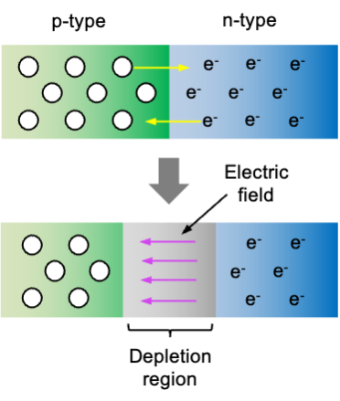
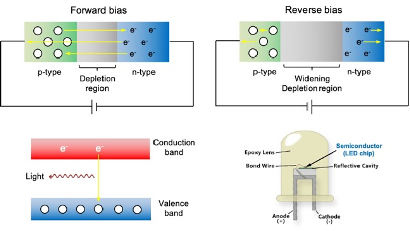
One advantage of MO theory is that it explains properties that earlier bonding models could not, such as the paramagnetism of oxygen molecules, where unpaired electrons are present in molecular orbitals. The theory also provides a quantum-mechanical explanation for the d-orbital splitting described in the ligand field theory, and sheds light on why many transition metal complexes are coloured. Finally, it is the foundation of band theory, which explains how semiconductors work.
In summary, molecular orbital theory describes chemical bonding by forming molecular orbitals from atomic orbitals, distributing electrons across the entire molecule, and using orbital energies and bond order to explain molecular stability and properties.